Re-timer circuits handle the waveform and noise reduction needed for high-density transmitter circuit and high-speed transmission signals. Because individual re-timer circuits are susceptible to coupling from adjacent ones, it has been difficult to lay them out in close proximity to each other. While the transmitter/receiver circuit width can be adjusted down to 0.25 mm, the typical pitch of laid out optical fibers, the re-timer circuit required a pitch of at least 0.5 mm.
By developing a mathematical model and analytic techniques for the impact of mutual coupling between re-timer circuits, Fujitsu Laboratories succeeded in laying out, for the first time in the world, re-timer circuits with spacing of just 0.25 mm, the same distance between optical fibers. This result enables optical transceiver circuits to integrate with high density.
In tests of this technology, transmission bandwidth of 100 Gbps (25Gbps x 4) was confirmed by running four lanes of an optical transceiver circuit with an integrated re-timer circuit and an optical device. Using this optical transceiver circuit with an integrated re-timer circuit and optical device in a 16-lane configuration will enable 400 Gbps next-generation interconnects, which can be utilized for data transmissions between future servers and the high-volume data transmissions of next-generation supercomputers.
Details of this technology are being presented at IEEE International Solid-State Circuits Conference 2015 (ISSCC 2015), opening February 22 in San Francisco (ISSCC presentation 22.7).
Background
As the performance of servers and supercomputers improves, and as virtual environments advance, the volume of data transmitted between servers and between CPUs is increasing. The capacity of optical interconnects between servers and between CPUs is also increasing, but because there are limits to the increases in speed that can be achieved using a single channel, there is a need for high density optical transceiver circuits that connect multiple channels.
Technological Issues
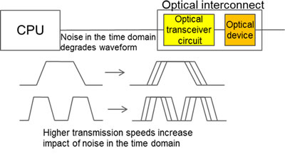
To increase transmission capacities, both higher speeds and higher densities are needed, but at higher speeds, noise is produced at the connection between the CPU and optical interconnect, leading to waveform degradation. Because noise that inhibits high-speed operation generates a phenomenon known as "jitter," which represents variance in the waveform in the time domain, the timing will be off when processing the signals (Figure 1).
To fix this, there is a need for overall high-density circuit technology that includes circuits that correct waveform degradation in the time domain. At present, while there are single integrated circuits that can drive multiple channels of optical devices, the re-timer circuits that correct the waveform in the time domain have their own high-speed oscillators, in which there are embedded coils. Because these produce mutual coupling, the re-timer circuits needed to be spaced at a distance of at least 0.5 mm from each other. This coupling has proven to be a significant obstacle to reducing sizes when attempting to integrate circuits for multiple channels.
 Figure 1: Noise in the time domain
About the Technology
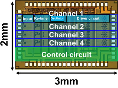
Fujitsu Laboratories has realized a circuit that reduces coupling between re-timer circuits, allowing for 0.25 mm spacing (Figure 2).
The technology has the following features:
1. Technology for analyzing the effects of mutual coupling on re-timer circuits
Fujitsu Laboratories has mathematically modeled the mutual coupling between the coils in the oscillators, coupling with complex behavior that had not been clarified until now. That model has been incorporated into a circuit simulator, and the impact of the operating noise on re-timer circuits has been quantified using simulations.
2. Eliminating the effects of mutual coupling between coils, enabling 0.25 mm pitch re-timer circuits
By comparing against simulation models, Fujitsu Laboratories identified approximately 10 design parameters that lowered the effects of mutual coupling between coils, and by varying each parameter calculated the optimal values. This led to the development of a gain-tuning circuit that adjusts the current amplification at a speed that can track the fluctuations caused by the coupling between re-timer circuits.
These advances together succeeded in reducing the pitch at which re-timer circuits can be laid out to 0.25 mm, from the previously required pitch of 0.5 mm or more. By enabling all of the components of the optical transceiver circuit, consisting of optical device, driver circuit for the optical device, and re-timer, to all be laid out at the same pitch, Fujitsu Laboratories was able to create a high-density optical transceiver.
 Figure 2: Prototype four-channel re-timer, integrated, optical transceiver chip
Results
In tests, transmission speeds of 100 Gbps were confirmed by running four parallel lanes of an optical transceiver circuit with an integrated re-timer circuit and an optical device. This technology makes it possible to miniaturize re-timer circuits and optical devices, enabling high-density optical interconnects. Using a re-timer circuit and optical device in a 16-lane configuration will enable 400 Gbps next-generation interconnects, which can be utilized for the high-volume data transmissions of next-generation supercomputers.
Future Plans
Fujitsu Laboratories is aiming to bring higher-capacity optical interconnects for servers into practical implementation in fiscal 2016, and is working to develop compact optical interconnect technology.

 O-Sense

.jpg)


.png)

